
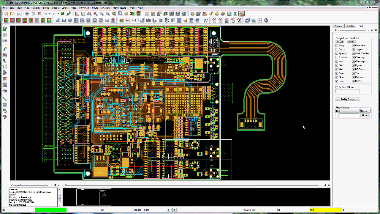
Find And Edit Objects In Pcb Design
Find the object which attribute is different than this attribute. Every faces significant challenges once a board gets overpopulated with and traces.
Why Move Up to Allegro 17.22016? Vince's Favorite
Up to 9% cash back editing multiple objects.
Find and edit objects in pcb design. In this case, this utility to find other objects would want to preserver the original find filter settings. This option only for the schematic, you can find the object for current sheet or all sheets. A query is essentially a description of something that you would like to find in the design data.
Community forums pcb design allegro pcb editor and pcb skill find filter issue. To clear the selection of the find similar objects use the shift + c hotkey. Alternatively, you can edit the properties of any object in the pcb inspector panel.
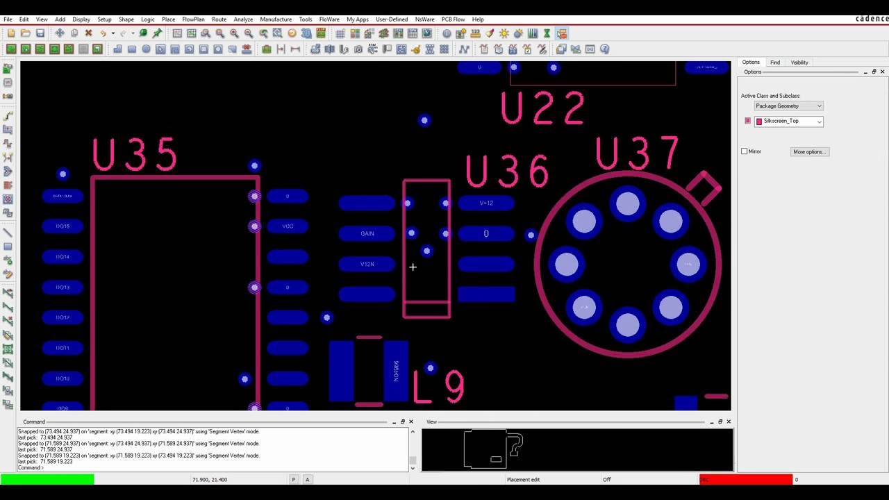
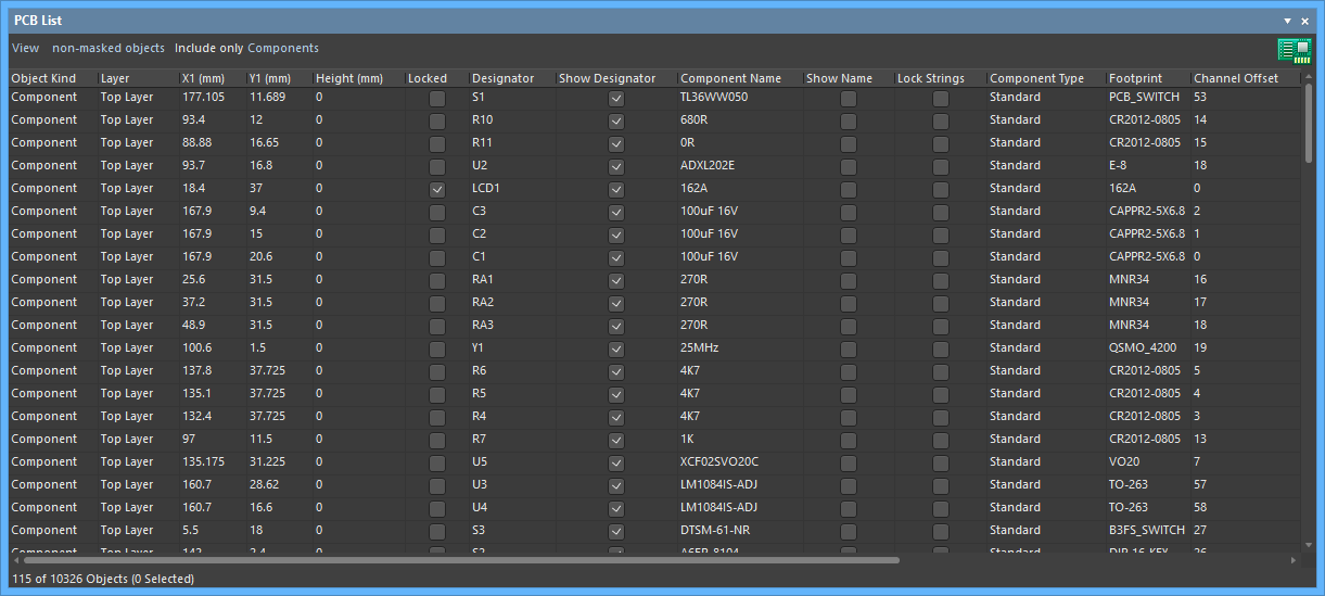
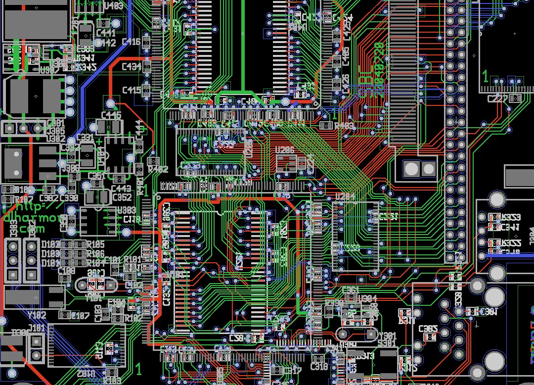
• object browser, this selection opens the find by name/property dialog Filtering to find the objects. It can be a great challenge for engineers to make edits to specific objects on overpopulated boards.
In pcb editor, your 3d canvas can include both pcb and enclosures. Only find the object which attribute same as this attribute. Read on to learn more.
Native 3d design means collisions and drcs get detected early—often in real time, during interactive layout. If you look at the status bar at the bottom of the pcb editor it holds the following information. Select all of your design using edit → select all → objects (ctrl+a), use the pick tool (arrow) to drag the image around to where you want it.
Another great feature is simultaneous 2d/3d design. Electronic design is the process of capturing a logical design in the schematic, then representing that design as a set of objects in the pcb workspace. Use the edit » find similar objects command from the main menus then click on an object in the workspace.
After performing the edit, you will probably find that all the other objects on the schematic are faded out, or masked. Easyeda pcb file object is a json object which allows you to hack your designs via another language, such as javascript, python, php, c, c++. You can query the design data in a number of different ways.
The find filter is optimized depending on the command and/or application mode you're currently in. Use pcb flow → 3. After they selected an object your code might need to find other objects using the find filter.
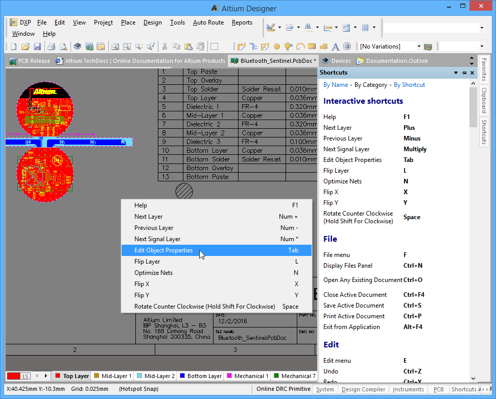
The pcb inspector panel enables you to interrogate and edit the properties of one or more design objects in the active pcb document. When used in conjunction with appropriate filtering, the panel can be used to make changes to multiple. Using a query to find and edit multiple objects.
Click view | pcb | to display the panel, then select the object to load its properties into the pcb inspector. Select the object to be placed from one of the toolbars or the place menu. This design is small with only a few components and therefore the outline is also small.
After that, by clicking on "edit", the following window will open showing the parameters of the currently selected object. The interesting thing is that your can control/modify your design in easyeda editor via javascript. Select the object what you want to find.
Mode changes to edit mode and a new blank sheet appears. While something is masked it cannot be edited, to remove the mask click the clear button at the bottom right of the workspace [shortcut: Press shift+f then click on an object in the workspace to use as the template.
From the start on, you can track your changes with different methods. Altium designer has a powerful query engine built into it, which is used to precisely target design objects. Select pcb objects and use the pcb filter panel to populate the pcb inspector panel with objects to be viewed or edited.
And find objects in the drawings. Leverage the global editing and custom query features in altium designer ® to easily locate objects and maintain consistency in your designs. The orcad and allegro pcb editor lets you create printed circuit board designs and.
Properties of the current object loaded into the find similar objects dialog. Via top menu > edit > find similar objects… kind: Use the mouse to define the location of the placed object in the pcb workspace and its size (where applicable).
Follow the below steps to place an object (component) on the pcb layout: Use step and repeat to duplicate. This object will be used as the template for finding similar objects.
Even for a small circuit, the schematic can include many. Version (v2.6) mar 10, 2008 1. It helps you in the whole development process.
There are 4 general options of editing objects: Outlines → draw/edit board outline 9. If the pcb design changes while the query dialog is active, the present query will.
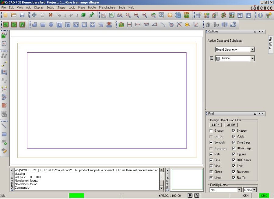
Getting Started with OrCAD PCB Designer Page 2 of 2

How to Find a Fault in a Circuit Board Techwalla
Placing and Editing PCB Objects Altium Designer 21 User

OrCAD PCB Designer Standard Special FlowCAD
Editing Multiple Objects Altium Designer 18.1 User
OrCAD PCB Designer file extensions
Placing and Editing PCB Objects Altium Designer 16.1
OrCAD PCB Designer Standard Special FlowCAD
Inkscape for pcb Growth Control Labs KnowledgeBase

Placing and Editing PCB Objects Altium Designer 21 User
Kicad Keyboard Shortcuts PCB Designs
Placing and Editing PCB Objects Altium Designer 21 User

Editing Similar PCB Objects Global Editing Altium
Orcad Pcb Designer Export Dxf PCB Designs
Circuit Board Drawing at GetDrawings Free download
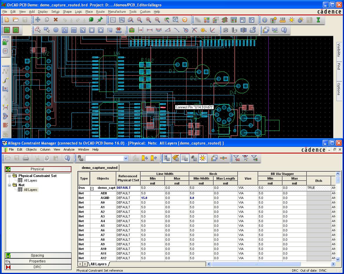
Tutorial Cadence OrCAD and Allegro PCB Editor Change

OrCAD Tutorial 2 Esplorare le librerie PCB, OrCAD PCB
Placing and Editing PCB Objects Altium Designer 16.0

pcb design How to edit dimensions for PCB layout in